On the surface, this article (https://lnkd.in/g8MrKDK6) may look like a technical article with technical implications.
The implications, though, go beyond technology, into arenas like geopolitics. In today’s era, nations and companies need to see technology through multiple lenses, in order to not only make the best use of it, but also to make sure that they do not get disrupted by it.
For those not familiar (I wasn’t till a couple of years ago), a simplified process for integrated circuits (e.g., CMOS chips) goes roughly like this:
Wafer preparation — start with an ultra-pure silicon (or compound) wafer.
- Oxidation — grow or deposit an oxide layer (e.g., SiO₂ or TiO₂) for insulation, passivation, or as a gate dielectric.
- Photolithography — use light + photoresist to pattern regions where changes should happen.
- Etching — remove unwanted material to define transistor shapes or diffusion windows.
Doping / Ion implantation — introduce dopant atoms (boron, phosphorus, arsenic, aluminum, etc.) to create n-type or p-type regions. - Annealing — heat treatment to repair crystal damage and activate dopants (make them electrically active).
- Deposition (CVD, PVD, ALD) — add thin films of metals, oxides, or nitrides for contacts, gates, or interconnects.
- Metallization & interconnect — form the wiring layers.
Passivation & packaging — seal and prepare for final device assembly.
The process is highly complex. Processes like oxidation and doping
normally take tens of hours, high-temperature vacuum treatments, and ion-implantation equipment.
But technology is on the path to simplifying these complex processes.
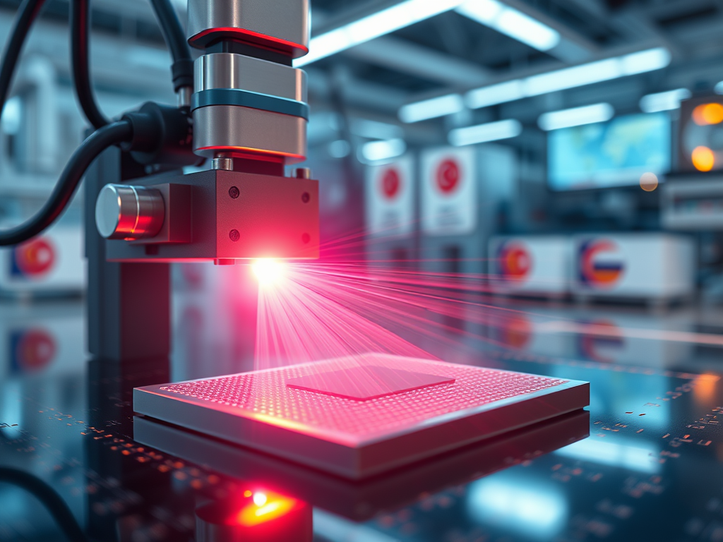
In this research, the researchers developed a technique called Laser-Induced Oxidation and Doping Integration (LODI), which uses a single laser irradiation step to simultaneously oxidize and dope a semiconductor material.
Specifically, they converted Titanium dioxide (TiO₂), which traditionally functions as an n-type semiconductor, into a p-type semiconductor (where holes rather than electrons are the majority carriers).
The process works by placing a thin layer of aluminium oxide (Al₂O₃) on titanium metal film, then laser-irradiating: aluminium ions diffuse in, titanium oxidizes to TiO₂, and the doping/oxidation together change the conductivity type.
The key benefit: what normally takes tens of hours, high-temperature vacuum treatments, and ion-implantation equipment is achieved in seconds with just one laser step.
While still early, the eventual result will be that the extremely high barrier to entry in the semiconductor industry will be reduced significantly.
Currently, this is the only barrier between some developed nations and those on the cusp of becoming developed or striving to do so. You see where I am going with this?
Almost every development in technology has implications beyond technology!
